And they usually meant what do you in front of a computer, outside of tweeting and posting on Facebook....
Well my job does indeed consists of
 |
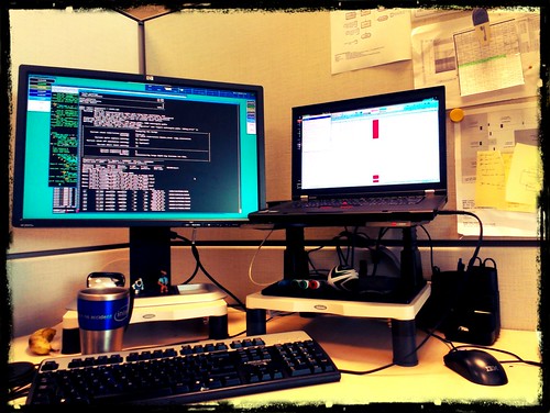
| My work station in the Irish office. |
First a bit of generic background on how electronic chips are made ( http://www.intel.com/about/companyinfo/museum/exhibits/sandtocircuits/index.htm ) :
As for my part the physical integration - or layout -, it does the translation of the system description in some programming language into a graphic representation (the layout) which will be used to produce the chip in the factory. Or: Chip design involves migrating a design from the logical realm (front-end design) to the
physical realm (back-end design).
The microelectronic chip are made of tiny - and getting tinier as the years passes - transistors, laid out on a silicon sheet. The process used involve photolithograhy - very similar to the development on photographic films - and used masks. Which masks I am helping creating.
 |
| An inverter and it's layout equivalent |
The job can also lead to some Chip Art. Sadly i have no pictures of the doodles I may or may not have inserted in past chips.
Since I moved to Digital stuff, where actually some program do layout the rectangles for you, and you're controlling those programs ( or trying to ). The idea here is to automate as much as possible the layout process, and ensuring the timing and other rules are respected.
The basic knowledge how mask design, and what are the physical impacts is still needed, but the tasks there are more programming or at least scripts writing, not too offense the software people.
Further reading on chip art:
- An interesting gallery online of these disappearing features: http://micro.magnet.fsu.edu/micro/gallery.html
- A IEEE Spectrum article on Chip Art:
http://spectrum.ieee.org/semiconductors/design/the-secret-art-of-chip-graffiti
- http://en.wikipedia.org/wiki/Physical_design_(electronics)
- http://en.wikipedia.org/wiki/Integrated_circuit_design
